Видео с ютуба Semiconductor Metallization

Metallization: Making Conductive Traces on Silicon Chips.

Molybdenum-Based Metallization: Unlocking New Economies of Scale in Semiconductor Manufacturing

Lam's ALTUS Halo: A New Era of Semiconductor Metallization for Molybdenum Atomic Layer Deposition

‘Semiconductor Manufacturing Process’ Explained | 'All About Semiconductor' by Samsung Semiconductor
![[Eng Sub] Wafer Bumping Process: Solder bump, Cu pillar bump, UBM](https://ricktube.ru/thumbnail/VLwqssWjRMU/mqdefault.jpg)
[Eng Sub] Wafer Bumping Process: Solder bump, Cu pillar bump, UBM

Silicon Wafer Processing | What You Need to Know About Metallization

Introduction to Chemical Mechanical Planarization/Polishing (CMP) in Semiconductor Fabrication

Advanced under-bump metallization (UBM) with the AP&S e-less tool Vulcanio

Why India can't make semiconductor chips 😱|UPSC Interview..#shorts

Metallization Introduction | Metallization | VLSI Technology | VLSI Fabrication
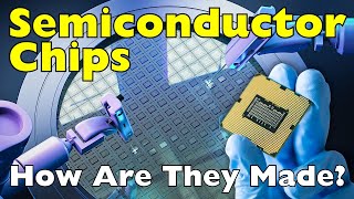
How Are Semiconductor Chips Made?
Eless plating wet bench Vulcanio for efficient UBM (under bump metallization)

Molybdenum (Mo) Has Lower Resistivity Than Tungsten

30 years of electroless plating for semiconductor and polymer micro-systems

반도체 제작기술 Metallization 리뷰

The World of Advanced Packaging

Hongfeng VAC Vacuum Multi Arc Ion Plating PVD Titanium Nitride(TiN) Gold Coating Machine

Introduction to SMART Metallization Lab

Metallization

PACKAGING SEMICONDUCTOR DISCRETE DEVICES